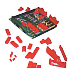
Chaitanya dip moulding works provides masking technique for pcb components. Pcb is the foundation of any electronic system. The present method of masking is done with the help of tape, which is very labourious and expensive apart from poor quality of job moreover these tapes are not reusable and leaves residual effects on components and pcb. At present the process of acrylic conformal coating takes about 3/4th of the complete processing time and major share of it consumed by masking and unmasking of connectors, some ics test points, contact points, potentiometers, trimmers, power transistors etc. Improper masking and unmasking also leads to damage/unplugging of ic, stray marks on pcb, residue marks on ic, stencil marks on ic get omitted etc.